Control Board
Control Board
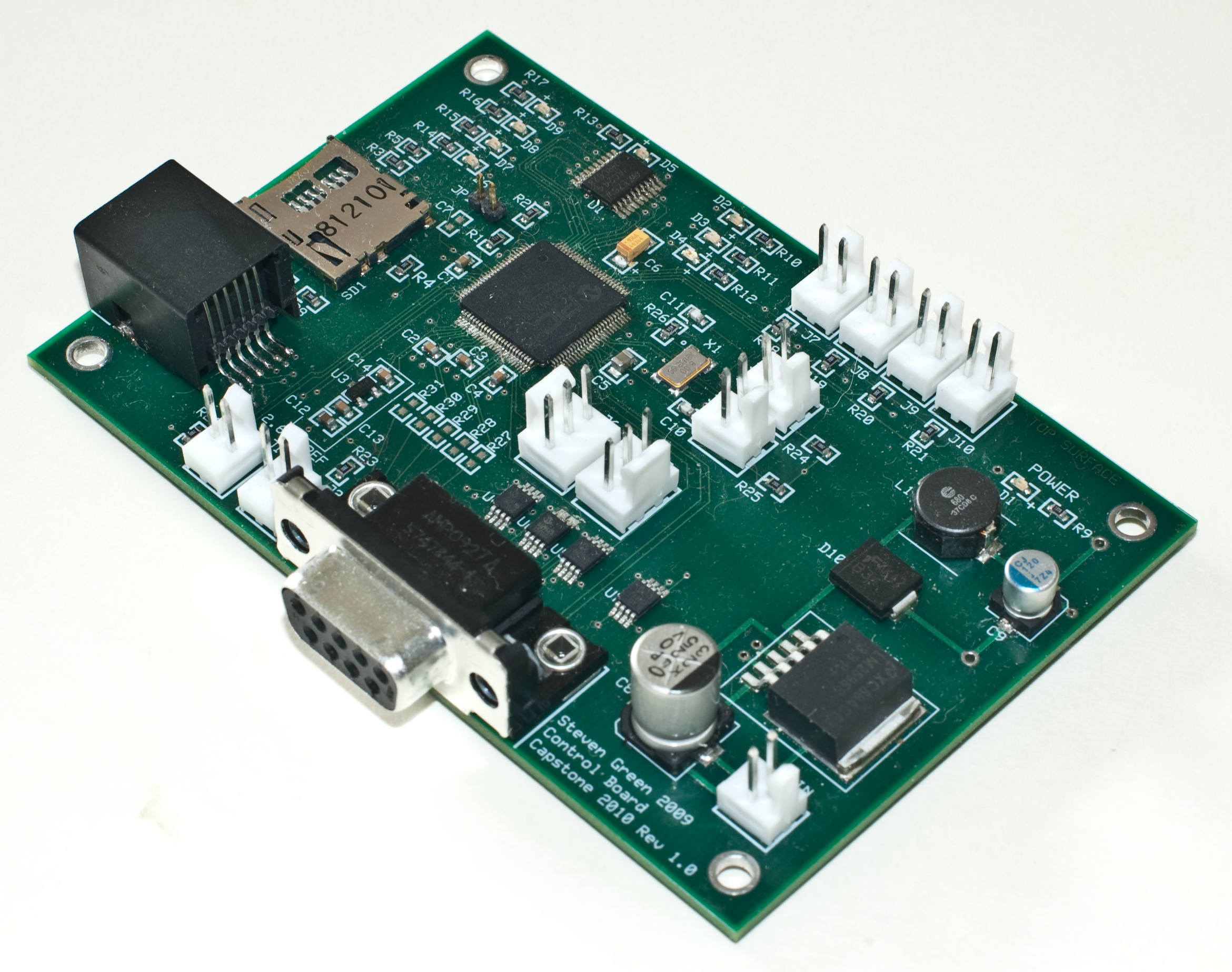
I designed a electro-mechanical platform to keep a camera level when mounted on a vehicle for my senior capstone project at UMass Lowell in 2010. The project required a control board to respond to sensor input and control linear actuators.The control board requirements:
- Programmable in C due to existing skills
- Sufficient memory for a small PID program
- High speed to process and respond to the sensors
- Matching connector to sensor board
- 2 Serial outputs to the motor controllers
- An on-board EEPROM to store calibration data (PID Gains)
- 5 analog to digital converters connections for the sensors
- SD memory card slot for recording logs and data
- Several LEDs to provide visual feedback
- An RJ-11 connector matching that provided by the Microchip ICD-3
- Powered input range up to 24V DC minimum to safely handle a vehicle source
- Headers for control switches
Due to existing skills it was beneficial to be able to write the firmware in C. In order to reduce the risks involving insufficient ram, processing speed and insufficient connectivity, and given that this initial prototype would be made in small quantities, a PIC micro-controller was chosen that was overkill for the application.
The processor chosen was a Microchip PIC32 processor in the 100-pin packaging. This processor provided a good combination processing power at 80MHz, and the most external connectivity of the PIC micro-controller family, 85 external connections, two UART serial outputs needed by the motor controller, and two SPI buses for communication with EEPROM, ADCs, and an SD card slot.
Overall design decisions and part selection was not made for cost reasons, rather, being a project on limited time and not expected to go beyond prototyping volume considerations were ignored. Had cost been an issue different micro-controllers would have been selected meeting the minimum needs of the project. These would include fewer pins, less ram, a slower processor, and reduced features.
The micro-controller contained ADCs; while the design that follows implemented these, higher bit-count ADCs external to the processor were added as a hedge against the resolution of internal ADCs. This duplication resulted in components for setting the voltage range on the micro-controller and additional ADCs; only one of the ADC sets would actually be required.
Design of the control board began with the circuits needed by the micro-controller itself. The Microchip datasheet provided a schematic of a typical implementation, shown in Figure 1.
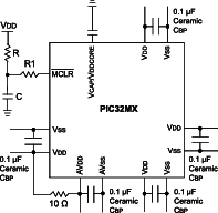
The circuit shown in Figure 1 provided many of the initial power connection requirements. This chip required \(3.3V DC\) source; this was a constant requirement of all the electrical components used, excluding the motors which would require higher voltages. Early options presented themselves from this schematic.
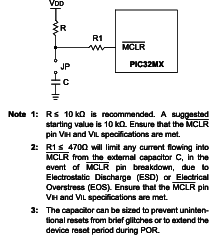
The MCLR pin is a processor reset. Capacitance could be added on this pin to prevent a sudden drop in voltage from resetting the controller. This pin causes issues with using an in-circuit debugger (Microchip’s ICD-3) as the micro-controller programmer. In order to enable the in circuit debugger (ICD) for development of the board jumper pins were added to the MCLR pin. This configuration is shown in Figure 2.
In Figure 1, The AVDD and AVSS pins provided a reference voltage used for ranging the analog to digital converters (ADC) on the controller. The AVDD voltage represents what would be a maximum 10-bit value by the internal ADCs and the AVSS would be the minimum, zero voltage. Selection of these values allows for greater resolutions, even with the 10-bit ADCs, since the range can be narrowed to the maximum range. Incorrect selection of these values could lead to clipping of the data or insufficient resolution. Seeking to maximize the sensitivity of the ADC the range was limited to \(0-2.6V\). If the sensors provide output in this range the resolution would be \(2.5mV/step\).
In order to use Microchip’s in-circuit debugger (ICD-3) as the programmer of the controller mounted to the circuit board, the following connections are needed, Figure 3.
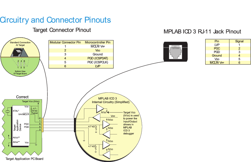
While not needed for normal operation, Figure 3 shows an oscillator. An external oscillator is needed for all the features of the debugger to be available. A 8MHz ceramic crystal oscillator was included for this reason.The power for the ICD-3 is provided by the target board. It was desired to be able to power the control board from the same source as the motors. At the time of the design, the motors were expected to run off between \(12V DC\) and \(24V DC\) source, directly from the car or a battery pack.
Since the control board requires \(3.3V DC\) the control board must step down the voltage. For efficiency and heat reasons, rather than use a voltage reference which would be simpler, a DC-DC converter was implemented. A safe estimate for total power required by the control board was less than 1 amp including LEDs, the sensor board, micro-controller and all the supporting chips. For a minimum voltage safely greater than \(24V DC\), a national instruments LM2595-3.3 power converter was selected. It could handle up to \(45V\) maximum input and output \(3.3V\). The data-sheet for this power converter provided a typical implementation shown in Figure 4.
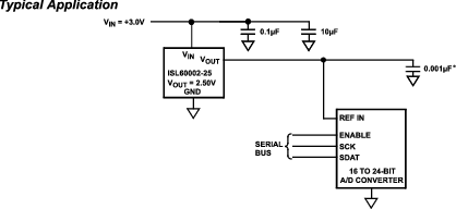
The schematic shown in Figure 4 was included in the design of the control board. Some of the parts used in this typical implementation were through hole parts, so comparable surface mount parts were selected. Additionally, not all the components used were rated to \(45V\). A capacitor on the supply side of the converter \(C_{in}\) is only rated to 35V resulting the maximum power supply being designed to \(35V DC\).The complete control board schematic, including the aforementioned features, is shown in the following schematic, Figure 5.
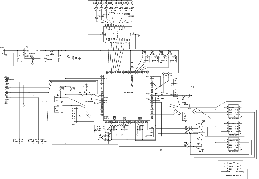
As shown in Figure 5, all the features specified to this point have been accounted for. The remaining components include 3 ADCs, an EEPROM, a bus driver “74AC244”, and a variety of external connectors.
The ADC converters, the EEPROM and the microSD card connector all communicated using the SPI bus with the micro-controller. The PIC32MX has two separate SPI buses (two separate sets of pins). Each bus can handle many peripherals. In this board design the microSD card connects to one SPI bus and the ADCs and EEPROM share the other bus. A chip select pin, a micro-controller digital output, is toggled in order to select a specific peripheral.
For file storage a microSD card was selected as it required the least amount of space on the circuit board. The SD card storage provides the opportunity to collect and store data, write output logs, and read configuration files. The files were stored using a FAT file system compatible with current personal computers. File system handling was programmed into the micro-controller in C.
An EEPROM provided a limited amount of static storage for PID calibration data.
Three 12-bit ADC ICs were connected. These IC chips are each handled two analog lines. Only five of the 6 available analog inputs are used: 3 intended for the accelerometer axes and 2 dedicated to the gyro axis, the extra ADC is tied to ground. All the analog signals came from a sensor board connected through a DB-9 connector.
In order to power LEDs a bus buffer was added. The buffer provides a method to power LEDs without putting strain on the micro-controller. The micro-controller can source and sink enough current to power a number of LEDs, however the buffer was a hedge against drawing too much current from the PIC. The LEDs provided visible feedback and status information from the software.
The remaining components were connectors to the micro-controller. There were three different types, external interrupt ports, digital inputs, and UART ports. The external interrupt ports, “J1, J2, J3 and J4”, were pulled high. When the circuit is closed these pins go to ground and invoke an interrupt in the micro-controller. This enables the controller to easily detect an external switch changes. The digital inputs, “J7, J8, J9, and J10”, provided additional external switches that did not generate interrupts, and could be polled. The remaining two connectors, “J5 and J6”, were used to provide UART communications. These two ports connected to third-party motor controllers.
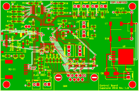
Three boards were fabricated by ExpressPCB. Due to the complexity of the board, the board was designed having four layers: two signal layers, and a power and a ground layer.The final board included changes not in the initial design following issues assembling the first copy. Due to the need for additional components the variety of LED colors shown in the schematic was replaced by a single color resulting in reduced cost and lower assembly time.
